- Engineering Excellence Without Compromise
Precision Capabilities for Complex PCB Designs
Our manufacturing capabilities are designed to meet the rigorous demands of modern electronics. We consistently invest in advanced processes and equipment to support intricate designs, specialized materials, and extremely tight tolerances. This is where your vision meets our technical precision.
Core Manufacturing Specifications
The following table outlines our standard and advanced manufacturing limits. Please contact our engineering team directly for projects exceeding these specifications.
| Max Layer Count: | 36 Layers (Standard) / 48+ (Advanced) |
| Min Trace Width/Spacing: | 3 mil / 3 mil |
| Aspect Ratio: | Up to 12:1 |
| Min Drill Size (Mechanical): | 0.15 mm |
| Surface Finishes: | ENIG, Immersion Tin, HASL (Lead-Free), ENEPIG, OSP |
Advanced PCB Technologies
High-Density Interconnect
Expertise in microvias, sequential lamination, and build-up layers for miniaturization and performance.
Rigid-Flex and Flex Circuits
Proven manufacturing of flexible and rigid-flex boards for dynamic applications.
High-Frequency/RF PCBs
Specialization in materials like Rogers and high-performance laminates for telecommunications and defense.
Heavy Copper PCBs
Supporting applications that require high current carrying capacity and thermal dissipation.
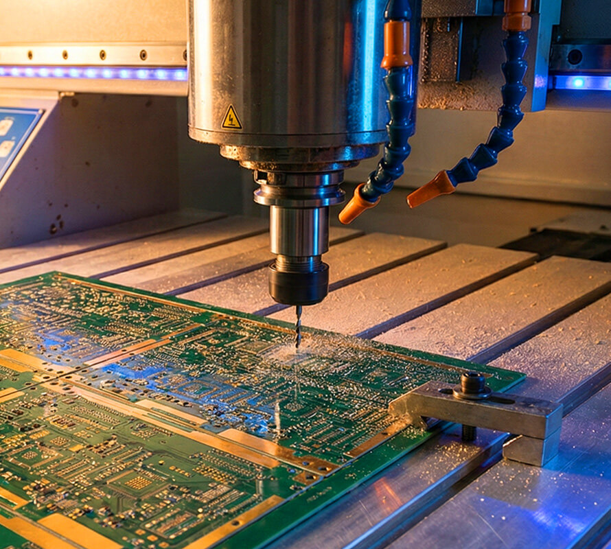
State-of-the-Art Equipment
Engineering Partnership and Custom Solutions
We work as an extension of your engineering team—turning complex requirements into production-ready solutions. From DFM guidance and prototyping to custom manufacturing support, we help optimize performance, cost, and reliability while meeting your exact specifications and timelines.